Scientists have developed electrically configured nanochannels that can eliminate unwanted energy waste and promise wave-based computing. This can revolutionize on-chip data communication and processing in future.
Conventional electronics is composed of logic circuits having a large number of transistors interconnected by metallic wires. The data carried by electric charges suffer undesirable heating limiting its integration density.
Spintronics, also known as spin electronics, or the study of the intrinsic spin of the electron and its associated magnetic moment, in addition to its fundamental electronic charge, in solid-state devices offer to harness electron spins. Their collective precession can carry information encoded in its amplitude, phase, wavelength, and frequency without any physical motion of particles, eliminating unwanted energy waste and promising wave-based computing.
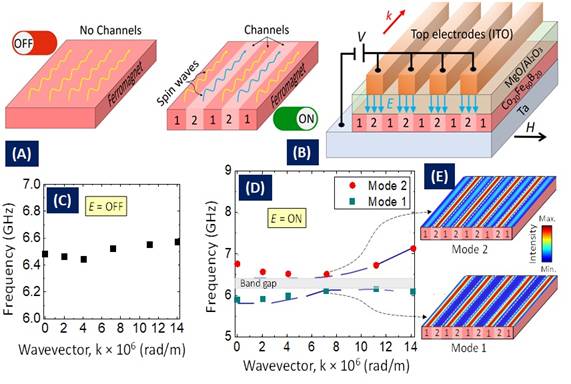
To this end, Professor Anjan Barman and coworkers from the S. N. Bose National Centre for Basic Sciences, an autonomous institute under the Department of Science and Technology (DST), Government of India, have developed electrically reconfigured parallel nanochannels that tune the behaviour of spin waves in nano-structure elements. They have done this by periodically tailoring the property that confers a preferred direction on the spin of a system, also called anisotropy using the electric field — technically called the principles of voltage-controlled magnetic anisotropy. This work has been published in the journal ‘Science Advances’.
In the recent research, spin-waves were efficiently transferred through these nanochannels, and this could be switched ‘ON’ and ‘OFF’ and its magnitude altered by a meagre voltage of few volts. The team believes that in future, these nanochannels can be engineered further to transfer specific bands of frequencies through designed parallel channels towards development of on-chip multiplexing devices.

Figure: A. Schematic illustration shows the concept of spin-wave nanochannels. B. Schematic illustration shows the device structure and formation of nanochannels. Spin-wave frequencies versus wavevector when electric field, E is OFF (C) and ON (D). E. Heatmap plots show the spatial distribution of spin-wave intensity for spin-wave mode 2 and mode 1 at wavevector k = 7.1 × 10⁶ rad/m.


